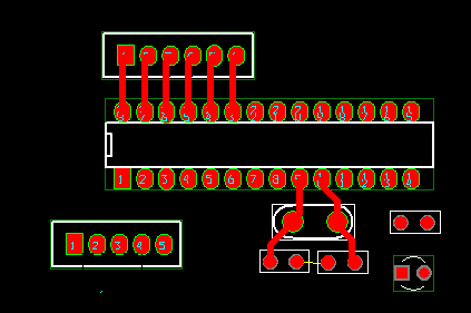
Now no need to design footprints when you design your PCB with any software
 |
footprints |
Now no need to design footprints when you design your pcb with any software!
Designing foot prints libraries is a long and tedious task!
you may be ready with your PCB design skills, but you can not make the serious peb design, until oyu don't have proper footprints!
Let's First understand -- What is the footprint?
Footprints, also known as land patterns, or Decal are an important aspect of PCB design as they define the physical layout of components on the board.
A footprint includes information such as the size and shape of the pads, the spacing between pads, and the location of any vias or through-holes.
Here are some reasons why footprints are important for a PCB designer:
1.Accuracy: Footprints must be accurate in order to ensure that components are placed correctly on the board and that they make proper electrical connections.
2.Assembly: The footprints must be designed in such a way that they can be easily assembled by automated machinery or by hand. The design should also take into account the needs of the assembly process, like the size and shape of the pads and the spacing between them.
Get (Total) 650 SMD+Desecrate components footprints made with ORCAD with just USD 99 ! OR ( INR rs. 7500)
( you can buy with this secure Paypal button. even you can pay using your card )
after you make purchase, the footprints .ZIP file will be immediately ready to download.
3.Reliability: Footprints must be designed to ensure that components are securely held in place and that the connections are reliable. This is particularly important for components that will be subject to vibration or other physical stresses.
4. Manufacturability: The footprints must be designed to be easily manufactured, taking into account the capabilities of the PCB fabrication process. This includes the size and shape of the pads and the spacing between them, as well as the location of any vias or through-holes.
5.Cost: The footprint design should take into account the costs associated with manufacturing and assembly, such as the size of the pads and the spacing between them, which can affect the cost of drilling and plating.
Therefore, as a PCB designer, paying attention to footprints is extremely important in order to ensure that the final product is accurate, reliable, and cost-effective.
--------------------------------------------------
What are the steps involved for creating new footprint for pcb design
Creating a new footprint for a PCB design involves several steps, including:
1. Researching the component: Before creating a new footprint, it's important to gather information about the component, such as its package type, dimensions, and pinout.
This information can be found in the component's datasheet or by searching online.
2. Designing the footprint: Once you have the necessary information, you can begin designing the footprint using PCB design software.
The footprint should include the size and shape of the pads, the spacing between pads, and the location of any vias or through-holes.
It's important to follow industry standards and guidelines for the footprint design, such as IPC-7351.
3. Verifying the footprint: Before using the new footprint in your design, it's important to verify that it is accurate and will work correctly with the component.
This can be done by creating a test board or by simulating the footprint in software.
4.Saving the footprint: Once the new footprint is verified, it should be saved in a library for future use. This library can be shared with other team members or with other projects.
5. Documenting the footprint: It is also important to document the footprint, including the component name, package type, dimensions, and any other relevant information.
This documentation should also include the date of creation and the name of the person who created the footprint.
Keep in mind that creating a new footprint can be a time-consuming process, and it's important to be thorough and pay attention to detail in order to ensure that the final product is accurate and reliable.
It's also important to keep in mind the PCB assembly process and manufacturability.
---------------------------------------------------
can foot prints imported in any pcb design software?
Yes, footprint libraries can be imported into most PCB design software.
The process may vary depending on the specific software being used, but generally involves opening the library file and adding the desired footprints to the current PCB design.
Some software may also allow for the creation of custom footprints within the program.
Most PCB design software support the import of footprint libraries in various file formats such as .lib, .mod, .kicad_mod, etc.
The process may vary depending on the specific software being used, but generally involves opening the library file and adding the desired footprints to the current PCB design.
====================================================================
Are you a PCB designer?
Are you struggling for foot prints ?
You want to start PCB designing at once and fast ?
Now no need to design footprints when you design your pcb with any software
you can start your design work Immediately after having these footprints!!
YOU CAN IMPORT THESE footprints in ANY PCB DESIGN SOFTWARE YOU USE !!
Get (Total) 650 SMD+Desecrate components footprints made with ORCAD with just USD 99 ! OR ( INR rs. 7500)
( you can buy with this secure Paypal button. even you can pay using your card )
after you make purchase, the footprints .ZIP file will be immediately ready to download.


No comments:
Post a Comment