

Function of OrCAD PCB Editor in the printed circuit board design process

The pcb design is the combination of art and technical.
You can say electronics is involved in learning pcb design but i have taught this beautiful and very productive art to many enthusiastic commerce students also !
The Electronics attached with pcb design is with high bond, but even you can say there is no much electronics knowledge needed for learning pcb design.
The Course offered by Teleview Electronics, is simply a 20 days course and any one can learn ( even non technical person ) PCB design in that period.
PCB design is a game of practice. the more practice you make, the more fluent you be and more easy for you to earn money out of pcb designing.
but the main condition is, you need to have dedication to leran pcb design to be successful.
herewith sharing something useful for PCB design learners to know how the things work in this short blog post.
you can always contact me to learn complete PCB design course and be proficient in only some months to earn a handsome amount daily by designing pcb's world wide.
-----------------------------------------------
By creating a digital description of the board layers for photo-plotters and CNC machines, which are used to create the boards, PCB Editor is used to design the PCB.
On the top, bottom, and all interior layers, copper traces are routed in separate layers, as are drill hole sizes and positions, solder-masks, silk screens, solder paste, part positioning, and board measurements.
In PCB Editor, these layers are not all depicted in the same way.
Some of the layers are presented from a positive angle, meaning that what you see with the program is what is added to the board, whilst other levels are presented from a negative angle, indicating that what you see with the software is what is subtracted from the board.
The layers represented in the positive view are the board outline, routed copper, silk screens, solder paste, and assembly information. The layers represented in the negative
view are drill holes and solder-masks.
Copper plane layers are handled in a special way, as described next.
Fig. 1 shows routed layers (top and bottom and an inner, for example)
that PCB Editor shows in the positive perspective.
The background is black and the traces and pads on each layer are a different color to make it easier to keep track of visually.
The drill holes are not shown because, the drilling process is a distinct step performed at a specific time during the manufacturing process.

figure 1. shows examples of drill symbols and silk screen representations
used by PCB Editor (traces not shown).
The red shapes (gray in print version) are examples of drill symbols that indicate locations of the drill holes and are used in conjunction with a drill chart (Fig. 1.19), which produces ID numbers for the different drill tools. The white print is the silk
screen.
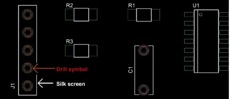
Circuit layout with drill symbols and silk screen on a
PCB.

fig.shows the solder-mask with the patterned holes that allow access to pads, and other Fig. shows the negative representation used by PCB Editor.
Here, the black background is actually the polymer film and the green circles (gray in print version) are the holes in the solder-mask.

Soldermask layer and negative view: (A) soldermask
and (B) negative view in PCB Editor
Plane layers may be processed as negative layers in PCB Editor and are
used to generate negative image Gerber files.
However, PCB Editor displays plane layers in the positive view.
Fig.A shows a physical copper plane layer with a thermal relief for a pin, Fig.B shows the negative view, and Fig. C shows the representation displayed by PCB
Editor in “what you see is what you get” mode.

Copper in a plane layer: (A) copper plane with
thermal relief, (B) negative view as processed, and (C) displayed in
WYSIWYG mode. WYSIWYG, What you see is what you get.
==================================================================


No comments:
Post a Comment